- 您现在的位置:买卖IC网 > Sheet目录473 > MAX2769BETI/V+T (Maxim Integrated)IC RCVR GPS UNIVERSAL 28TQFN
�� �
�
�MAX2769B�
�Universal� GPS� Receiver�
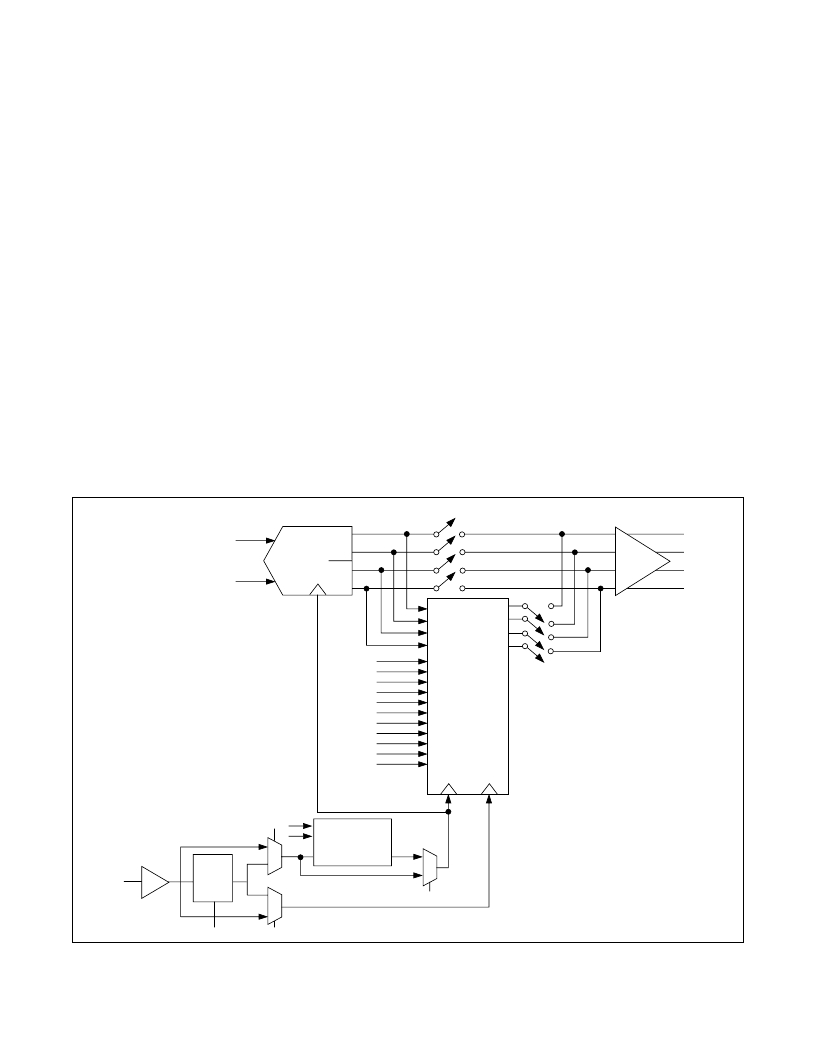
�DSP� Interface�
�GPS� data� is� output� from� the� ADC� as� the� four� logic� signals�
�(bit� 0� ,� bit� 1� ,� bit� 2� ,� and� bit� 3� )� that� represent� sign/magnitude,�
�unsigned� binary,� or� two’s� complement� binary� data� in�
�the� I� (bit� 0� and� bit� 1� )� and� Q� (bit� 2� and� bit� 3� )� channels.� The�
�resolution� of� the� ADC� can� be� set� up� to� 3� bits� per� channel.�
�For� example,� the� 2-bit� I� and� Q� data� in� sign/magnitude�
�format� is� mapped� as� follows:� bit� 0� =� I� SIGN� ,� bit� 1� =� I� MAG� ,�
�bit� 2� =� Q� SIGN� ,� and� bit� 3� =� Q� MAG� .� The� data� can� be� serial-�
�ized� in� 16-bit� segments� of� bit� 0� ,� followed� by� bit� 1� ,� bit� 2� ,� and�
�bit� 3� .� The� number� of� bits� to� be� serialized� is� controlled� by�
�the� bits� STRMBITS� in� the� Configuration� 3� register.� This�
�selects� between� bit� 0� ;� bit� 0� and� bit� 1� ;� bit� 0� and� bit� 2� ;� and�
�bit� 0� ,� bit� 1� ,� bit� 2� ,� and� bit� 3� cases.� If� only� bit� 0� is� serialized,� the�
�data� stream� consists� of� bit� 0� data� only.� If� a� serialization� of�
�bit� 0� and� bit� 1� (or� bit� 2� )� is� selected,� the� stream� data� pattern�
�consists� of� 16� bits� of� bit� 0� data� followed� by� 16� bits� of� bit� 1�
�(or� bit� 2� )� data,� which,� in� turn,� is� followed� by� 16� bits� of� bit� 0�
�data,� and� so� on.� In� this� case,� the� serial� clock� must� be� at�
�least� twice� as� fast� as� the� ADC� clock.� If� a� 4-bit� serialization�
�of� bit� 0� ,� bit� 1� ,� bit� 2� ,� and� bit� 3� is� chosen,� the� serial� clock� must�
�be� at� least� four� times� faster� than� the� ADC� clock.�
�The� ADC� data� is� loaded� in� parallel� into� four� holding�
�registers� that� correspond� to� four� ADC� outputs.� Holding�
�registers� are� 16� bits� long� and� are� clocked� by� the� ADC�
�clock.� At� the� end� of� the� 16-bit� ADC� cycle,� the� data� is�
�transferred� into� four� shift� registers� and� shifted� serially� to�
�the� output� during� the� next� 16-bit� ADC� cycle.� Shift� regis-�
�ters� are� clocked� by� a� serial� clock� that� must� be� chosen�
�fast� enough� so� that� all� data� is� shifted� out� before� the� next�
�set� of� data� is� loaded� from� the� ADC.� An� all-zero� pattern�
�follows� the� data� after� all� valid� ADC� data� are� streamed�
�to� the� output.� A� DATASYNC� signal� is� used� to� signal� the�
�beginning� of� each� valid� 16-bit� data� slice.� In� addition,�
�there� is� a� TIME_SYNC� signal� that� is� output� every� 128� to�
�16,384� cycles� of� the� ADC� clock.�
�STRM_EN�
�ADC�
�I�
�Q�
�DATA_OUT�
�BIT� 0�
�CLK_SER�
�BIT� 1�
�BIT� 2�
�DATA_SYNC�
�BIT� 3�
�TIME_SYNC�
�STRM_EN�
�STRM_START�
�STRM_EN�
�OUTPUT�
�DRIVER�
�PIN� 21�
�PIN� 20�
�PIN� 17�
�PIN� 18�
�STRM_STOP�
�CONTROL�
�SIGNALS�
�FROM� 3-WIRE�
�INTERFACE�
�STRM_COUNT<2:0>�
�DIEID<1:0>�
�STRM_BITS<1:0>�
�FRM_COUNT<27:0>�
�STAMP_EN�
�DAT_SYNCEN�
�TIME_SYNCEN�
�STRM_RST�
�CLK_ADC�
�CLK_SER�
�ADCCLK_SEL�
�L_CNT<11:0>�
�M_CNT<11:0>�
�REF/XTAL�
�PIN� 15�
�THROUGH�
�/2�
�/4�
�CLK_IN�
�CLK_OUT�
�x2�
�REFDIV<1:0>�
�SERCLK_SEL�
�FRCLK_SEL�
�Figure� 3.� DSP� Interface� Top-Level� Connectivity� and� Control� Signals�
�Maxim� Integrated�
�16�
�发布紧急采购,3分钟左右您将得到回复。
相关PDF资料
MAX2769EVKIT+
KIT EVAL FOR MAX2769
MAX2821ETM+T
IC TXRX 802.11B 2.4GHZ 48-TQFN
MAX2829EVKIT
EVAL KIT MAX2828, MAX2829
MAX2830EVKIT+
KIT EVAL FOR MAX2830
MAX2831EVKIT+
KIT EVAL FOR MAX2831
MAX2837EVKIT+
KIT EVAL FOR MAX2837
MAX2838EVKIT+
KIT EVAL FOR MAX2838
MAX2839ASEVKIT+
KIT EVAL FOR MAX2839A WLP
相关代理商/技术参数
MAX2769BEVKIT#
功能描述:射频接收器 Eval Kit for MAX2769B Universal GNSS receiver RoHS:否 制造商:Skyworks Solutions, Inc. 类型:GPS Receiver 封装 / 箱体:QFN-24 工作频率:4.092 MHz 工作电源电压:3.3 V 封装:Reel
MAX2769E/W
功能描述:射频接收器 RoHS:否 制造商:Skyworks Solutions, Inc. 类型:GPS Receiver 封装 / 箱体:QFN-24 工作频率:4.092 MHz 工作电源电压:3.3 V 封装:Reel
MAX2769E/W-GB6
功能描述:射频接收器 RoHS:否 制造商:Skyworks Solutions, Inc. 类型:GPS Receiver 封装 / 箱体:QFN-24 工作频率:4.092 MHz 工作电源电压:3.3 V 封装:Reel
MAX2769E/W-T
功能描述:射频接收器 RoHS:否 制造商:Skyworks Solutions, Inc. 类型:GPS Receiver 封装 / 箱体:QFN-24 工作频率:4.092 MHz 工作电源电压:3.3 V 封装:Reel
MAX2769E/W-TGB6
功能描述:射频接收器 RoHS:否 制造商:Skyworks Solutions, Inc. 类型:GPS Receiver 封装 / 箱体:QFN-24 工作频率:4.092 MHz 工作电源电压:3.3 V 封装:Reel
MAX2769ETI+
功能描述:射频接收器 Universal GPS Receiver
RoHS:否 制造商:Skyworks Solutions, Inc. 类型:GPS Receiver 封装 / 箱体:QFN-24 工作频率:4.092 MHz 工作电源电压:3.3 V 封装:Reel
MAX2769ETI+T
功能描述:射频接收器 Universal GPS Receiver
RoHS:否 制造商:Skyworks Solutions, Inc. 类型:GPS Receiver 封装 / 箱体:QFN-24 工作频率:4.092 MHz 工作电源电压:3.3 V 封装:Reel
MAX2769EVKIT+
功能描述:GPS开发工具 MAX2769 Eval Kit RoHS:否 制造商:STMicroelectronics 产品:Evaluation Boards 工具用于评估:IT600, STM32F20x 频率:1.575 GHz 工作电源电压:1.8 V 接口类型:Wireless